

Silicon Carbide Vacuum Chuck The Key Component in Semiconductor Manufacturing
Release time:
2024-09-26 00:00
Source:

In the field of semiconductor manufacturing, extremely thin wafers are placed on the silicon carbide vacuum chuck. This crucial component, connected to a vacuum generator, firmly fixes the wafers through vacuum suction.
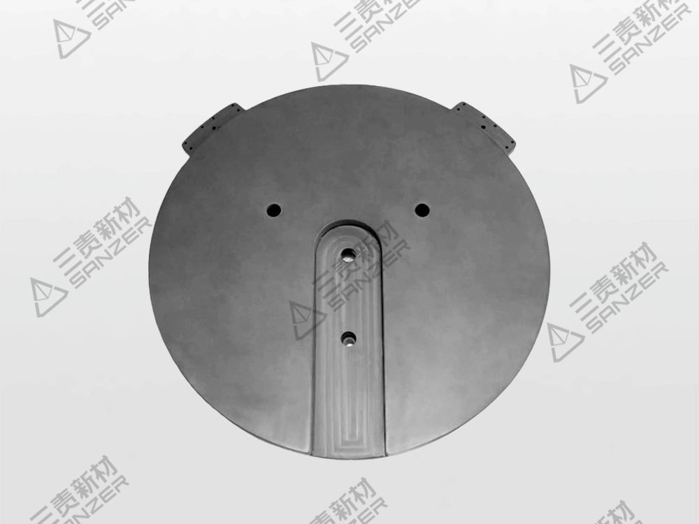
The silicon carbide vacuum chuck is widely used in various processes such as lithography, etching, laser processing, and wafer inspection. It exhibits several remarkable characteristics and advantages. It has precise dimensions and excellent thermal stability, ensuring accurate processing. It also has good thermal conductivity, a small expansion coefficient, and superior temperature uniformity performance.
Moreover, the silicon carbide vacuum chuck has extremely high wear resistance and a smooth surface finish. It has small and evenly distributed pores, enabling uniform adsorption of all areas of the wafer. It also possesses outstanding resistance to acid and alkali corrosion and can withstand plasma impact.
In terms of specifications, it can be custom-processed according to the customer’s drawings. The silicon carbide vacuum chuck plays an indispensable role in semiconductor manufacturing, providing reliable support for the production of high-quality semiconductor devices with its unique properties and advantages. With the continuous development of the semiconductor industry, the importance of the silicon carbide vacuum chuck will continue to increase, and it will continue to contribute to the progress of this critical field. Repeatedly, the silicon carbide vacuum chuck proves its value in ensuring the smooth operation and high efficiency of semiconductor manufacturing processes.
Key words:
Related News
Sanzer New Materials at CIBF in Shenzhen, 16-18 May 2023
May 16-18, the 15th China International Battery Fair was held at Shenzhen International Convention and Exhibition Center, which is one of the world's largest battery industry events, attracting more than 2,500 companies from around the world, with well-known companies in the battery industry chain gathering to share the development of new technologies and new trend.
Sanzer New Materials at Ceramics Expo in Michigan, 1-3 May 2023
From May 1st to May 3rd, SANZER participated in the Ceramics Expo to explore the American market. The exhibition is the largest and most influential industrial ceramics and refractories exhibition in the United States.
Sanzer New Materials at the 2nd Advanced Ceramics Summit Forum
On April 21, the second Advanced Ceramics Summit Forum was held in Nanchang, Jiangxi, co-sponsored by JOURNAL OF ADVANCED CERAMICS and Modern Technical Ceramics editorial department. Sanzer New Materials was invited to attend and discussed with experts and scholars in the powder and ceramic industry about the future development of structural ceramics.
Sanzer New Materials at the 7th Power Lithium Battery Cathode Material Summit, 12 July, 2022
Sanzer New Materials Attend the 7th Power Lithium Battery Cathode Material Summit
Sanzer New Materials participated in the "2021 Flow Chemistry Technology Research and Green Process Application Exchange Seminar" held in Jinan from July 24th to July 25th, 2021, and delivered the "SANZER Coresic ® The report on the development and application of silicon carbide ceramics in continuous flow microchannel reactors has attracted widespread attention and response
Sanzer New Materials at the 14th Shanghai Advanced Ceramics Exhibition
Sanzer New Materials participated in the Shanghai Advanced Ceramics Exhibition, which showcased the company's pressureless sintered silicon carbide ceramic products developed in recent years
Consultation hotline:
Address:No.99 East Changxing Road, Nantong Economic and Technological Development Zone, Jiangsu
Email:market@sanzer.com
Fax:86 21 5954 9392
Website:www.sanzer.com
WeChat Public Number
Enterprise WeChat
WeChat Public Number
Copyright©2022 Jiangsu Sanzer New Materials Technology Co., Ltd. 沪ICP备XXXXXXXX号 SEO Power by:www.300.cn


